- 您现在的位置:买卖IC网 > Sheet目录396 > AUIRFR4105ZTR (International Rectifier)MOSFET N-CH 55V 30A DPAK
AUIRFR/U4105Z
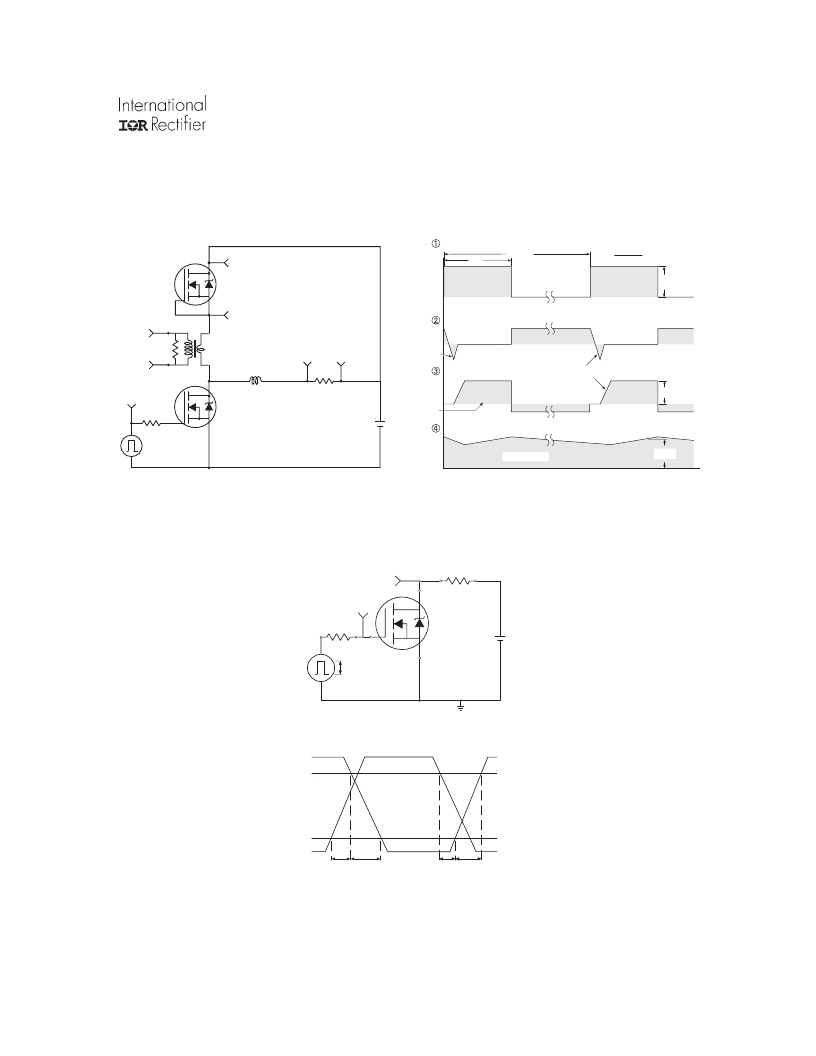
D.U.T
+
Driver Gate Drive
P.W.
Period
D=
P.W.
Period
+
?
-
Circuit Layout Considerations
? Low Stray Inductance
? Ground Plane
? Low Leakage Inductance
Current Transformer
D.U.T. I SD Waveform
V GS =10V *
D.U.T. V DS Waveform
?
?
-
R G
- ? +
? dv/dt controlled by R G
? Driver same type as D.U.T.
? I SD controlled by Duty Factor "D"
? D.U.T. - Device Under Test
V DD
+
-
Reverse
Recovery
Current
Re-Applied
Voltage
Inductor Curent
Body Diode Forward
Current
di/dt
Diode Recovery
dv/dt
Body Diode Forward Drop
V DD
Ripple ≤ 5%
I SD
*
V GS = 5V for Logic Level Devices
Fig 17. Peak Diode Recovery dv/dt Test Circuit for N-Channel
HEXFET ? Power MOSFETs
V DS
R D
- V DD
R G
V GS
D.U.T.
+
10V
Pulse Width ≤ 1 μs
Duty Factor ≤ 0.1 %
Fig 18a. Switching Time Test Circuit
V DS
90%
10%
V GS
t d(on)
t r
t d(off)
t f
Fig 18b. Switching Time Waveforms
www.irf.com
9
发布紧急采购,3分钟左右您将得到回复。
相关PDF资料
AUIRLR024NTR
MOSFET N-CH 55V 17A DPAK
AUIRLR2703TR
MOSFET N-CH 30V 20A DPAK
AUIRLR3410
MOSFET N-CH 100V 17A DPAK
AW24MUFL-H2
2.4GHZ WIRELESS MODULE U.FL
AWAC24U
2.4GHZ WIRELESS USB DONGLE
AWS24S
MODULE WIRELESS USB EXT ANT
B1A-10PK
LAMP INDICATOR T-3 1/4 120V 10PK
B2A
LAMP NEON T3-1/4 MINI BAYONT
相关代理商/技术参数
AUIRFR4105ZTRL
功能描述:MOSFET AUTO 55V 1 N-CH HEXFET 24.5mOhms RoHS:否 制造商:STMicroelectronics 晶体管极性:N-Channel 汲极/源极击穿电压:650 V 闸/源击穿电压:25 V 漏极连续电流:130 A 电阻汲极/源极 RDS(导通):0.014 Ohms 配置:Single 最大工作温度: 安装风格:Through Hole 封装 / 箱体:Max247 封装:Tube
AUIRFR4105ZTRR
功能描述:MOSFET AUTO 55V 1 N-CH HEXFET 24.5mOhms RoHS:否 制造商:STMicroelectronics 晶体管极性:N-Channel 汲极/源极击穿电压:650 V 闸/源击穿电压:25 V 漏极连续电流:130 A 电阻汲极/源极 RDS(导通):0.014 Ohms 配置:Single 最大工作温度: 安装风格:Through Hole 封装 / 箱体:Max247 封装:Tube
AUIRFR4292
制造商:International Rectifier 功能描述:"AUTOMOTIVE LOGIC LEVEL MOSFET 250V, 9.3A, 375 MOHM, 13 NC Q - Rail/Tube 制造商:International Rectifier 功能描述:MOSFET N CH 250V 9.3A DPAK 制造商:International Rectifier 功能描述:Automotive Logic Le mOhm, 13 nC Qg, DPAK
AUIRFR4292TR
制造商:International Rectifier 功能描述:"AUTOMOTIVE LOGIC LEVEL MOSFET 250V, 9.3A, 375 MOHM, 13 NC Q - Tape and Reel 制造商:International Rectifier 功能描述:MOSFET N CH 250V 9.3A DPAK 制造商:International Rectifier 功能描述:Automotive Logic Le mOhm, 13 nC Qg, DPAK
AUIRFR4292TRL
制造商:International Rectifier 功能描述:"AUTOMOTIVE LOGIC LEVEL MOSFET 250V, 9.3A, 375 MOHM, 13 NC Q - Tape and Reel 制造商:International Rectifier 功能描述:MOSFET N CH 250V 9.3A DPAK 制造商:International Rectifier 功能描述:Automotive Logic Le mOhm, 13 nC Qg, DPAK
AUIRFR4292TRR
功能描述:MOSFET Automotive Power MOSFET; 250V 345mOhm RoHS:否 制造商:STMicroelectronics 晶体管极性:N-Channel 汲极/源极击穿电压:650 V 闸/源击穿电压:25 V 漏极连续电流:130 A 电阻汲极/源极 RDS(导通):0.014 Ohms 配置:Single 最大工作温度: 安装风格:Through Hole 封装 / 箱体:Max247 封装:Tube
AUIRFR4615
功能描述:MOSFET AUTO 150V 1 N-CH HEXFET 42mOhms RoHS:否 制造商:STMicroelectronics 晶体管极性:N-Channel 汲极/源极击穿电压:650 V 闸/源击穿电压:25 V 漏极连续电流:130 A 电阻汲极/源极 RDS(导通):0.014 Ohms 配置:Single 最大工作温度: 安装风格:Through Hole 封装 / 箱体:Max247 封装:Tube
AUIRFR4615
制造商:International Rectifier 功能描述:N CH MOSFET AUTOMOTIVE 150V 33A TO-2 制造商:International Rectifier 功能描述:N CH MOSFET, AUTOMOTIVE, 150V, 33A, TO-252
